Free download.
Book file PDF easily for everyone and every device.
You can download and read online Growing Graphene on Semiconductors file PDF Book only if you are registered here.
And also you can download or read online all Book PDF file that related with Growing Graphene on Semiconductors book.
Happy reading Growing Graphene on Semiconductors Bookeveryone.
Download file Free Book PDF Growing Graphene on Semiconductors at Complete PDF Library.
This Book have some digital formats such us :paperbook, ebook, kindle, epub, fb2 and another formats.
Here is The CompletePDF Book Library.
It's free to register here to get Book file PDF Growing Graphene on Semiconductors Pocket Guide.
Graphene, the wonder material of the 21st century, is expected to play an important role in future nanoelectronic applications, but the only way to achieve this goal is to grow graphene directly on a semiconductor, integrating it in the chain for.
Table of contents
- Graphene integration with nitride semiconductors for high power and high frequency electronics
- Direct Growth of Graphene on a SiGe Alloy Surface by Chemical Vapor Deposition
- MIT News Office
- Growing Graphene on Semiconductors by Nunzio Motta, Hardcover | Barnes & Noble®
Advanced Nanomaterials for Aerospace Applications has been developed for a community interested in space science and nanotechnology. View Product. C Buckminsterfullerene: Some Inside Stories. This compendium of accounts reveals the unique perspectives of many scientists who made major contributions This compendium of accounts reveals the unique perspectives of many scientists who made major contributions to the Nobel Prize-winning discovery of C60 buckminsterfullerene but who have not previously published personal accounts.
The introduction attempts to provide a rational framework for Among nanomaterials, CdTe holds special technological importance as the only known II—VI material that can form conventional Carbon-based Nanomaterials and Hybrids: Synthesis, Properties,.
- 1st Edition.
- Direct Growth of Graphene on Silicon by Metal-Free Chemical Vapor Deposition.
- The Lost Fedora.
- Water Goddess.
- Viewpoint: Graphene Gets a Good Gap!
- The World of the Livings!
- Growing Graphene on Semiconductors!
In recent decades nanotechnology has developed into a highly multidisciplinary topic, drawing from a number In recent decades nanotechnology has developed into a highly multidisciplinary topic, drawing from a number of fields such as physics, materials science, biomedicine, and different engineering disciplines. The success of nanoscience- and nanotechnology-related research and products is connected with the Present-day computers lack well-defined functions to accept various kinds of sensual information such as vision, Present-day computers lack well-defined functions to accept various kinds of sensual information such as vision, hearing, and smelling binding problem.
Computers also lack any well-defined mechanisms to coordinate various behaviors in the presence of an object conscious mechanism. This book Dancing with Light: Advances in Photofunctional. Liquid crystal LC displays dominating in the present market of flat panel displays are generally Liquid crystal LC displays dominating in the present market of flat panel displays are generally based on interactions of light and LCs. Recent progress in this field indicates that integrating photochromic molecules into LC materials enables one to photomanipulate unique Functionalization of Molecular Architectures: Advances and.
Low-dimensional compounds are molecules that correspond to various shapes, such as rod, ladder one-dimensional compounds , Low-dimensional compounds are molecules that correspond to various shapes, such as rod, ladder one-dimensional compounds , and sheet two-dimensional compounds.
Graphene integration with nitride semiconductors for high power and high frequency electronics
They are ordinarily found in electromagnetic fields. Recently, versatile low-dimensional compounds were proposed for use as components of various Gallium Nitride Power Devices. GaN is considered the most promising material candidate in next-generation power device applications, owing to GaN is considered the most promising material candidate in next-generation power device applications, owing to its unique material properties, for example, bandgap, high breakdown field, and high electron mobility. Have doubts regarding this product?
Post your question. Safe and Secure Payments. Easy returns.
Direct Growth of Graphene on a SiGe Alloy Surface by Chemical Vapor Deposition
You might be interested in. Back to top. In addition, in-plane propagation, edge-propagation, and core-propagation processes were proposed to evaluate the sequentially changing graphene domains. A better understanding of the direct nucleation and growth mechanisms may enable the synthesis of large-area and layer-controlled, high-quality graphene on single-crystal silicon substrates. Skip to main content Skip to sections. Advertisement Hide. Download PDF. Nano-Micro Letters April , Cite as.
MIT News Office
Open Access. First Online: 08 December Abstract The metal-free synthesis of graphene on single-crystal silicon substrates, the most common commercial semiconductor, is of paramount significance for many technological applications. Open image in new window. A custom-made, portable chamber with a ceramic wafer was used as the heating platform Fig. A detailed description of the chamber is also presented in our previous report [ 35 ]. The silicon substrate is mounted face down on the heating stage with a narrow gap between the Si and the heating stage.
Unlike a commercial CVD chamber for graphene growth, the special design of the chamber used in this work remarkably increases the local concentration of hydrocarbon radicals and C ions, and enhances interaction with the silicon surface when the substrate is placed upside-down. Moreover, the confined hydrocarbon radicals and the increased collision frequency in the narrow gap further facilitate the nucleation of graphene [ 36 ].
This assumed mechanism is reasonable because the graphene was only observed on the upside-down surface. On the other hand, conventionally placed substrates cannot produce graphene or carbon nucleation at comparable temperatures. The graphene grains show a clear contrast difference with the silicon surface, and most of the grains exhibit a regular, hexagon-derived shape, similar to the single-crystal graphene on BN or Si 3 N 4 substrates [ 27 , 31 ].
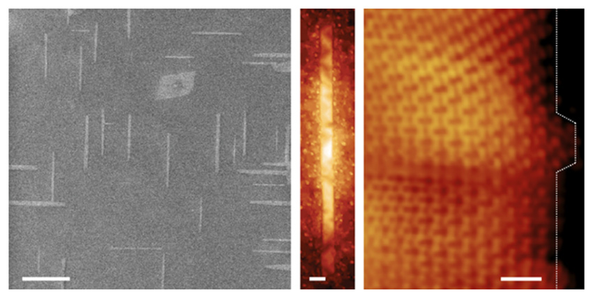
The high-magnification AFM topography and phase image Fig. These were confirmed by the height profiles shown at the bottom of Fig. This is accompanied by larger domain sizes as shown in Fig. Moreover, only a few core-bulging graphene domains small convex spots on the center emerge, which are marked by a red circle. The concave surface still dominates among the graphene grains.
Spectroscopic characterizations were further conducted to probe the microstructural changes in graphene for different growth temperatures. This spectrum has been fitted with several peaks assigned to sp 2 carbon The dominant peak of the sp 2 feature confirms the presence of graphene.
The C—H sp 3 carbon signal should be due to the H-terminated graphene edges, which is consistent with the Raman spectra in Fig. The Si—O peak is the result of the oxidization of silicon. The oxidization should have occurred only after the silicon substrate was exposed to air because the sample was annealed in a reducing atmosphere. We found that the intensity of the Si—Si peak increases with increasing growth temperature. This should be due to the increasing coverage of the graphene region because graphene prevents the oxidation of Si in air.
The lack of the Si—C peak at approximately Contrary to the observations of Hackley and Trung [ 32 , 33 ], the lack of the Si—C peak should be due to the following reason. In our CVD system, carbon is produced by the pyrolysis of methane. Without metallic catalysts, only a small number of C ions with weak mobility and activity were produced. Therefore, they would not react with silicon unless under much higher temperature, as demonstrated by Ki-Bum Kim et al.
The temperature-dependent structure of graphene was further evaluated by Raman spectroscopy, as shown in Fig.
This suggests the layer propagation of graphene domains, which is consistent with our AFM observations. Based on the above experiments, an integrated growth model considering the nucleation and growth process is proposed. In the first stage, due to the catalytically inert nature of silicon, the thermal self-decomposition of methane produces active carbon species that initiate graphene nucleation Fig. Due to the upside-down-placed substrate, the super-saturation of carbon radicals and high collision frequency promotes the anchoring of carbon atoms onto the silicon surface and facilitates graphene nucleation.
It was also reported that the high density of dangling bonds on a silicon surface could enhance nucleation [ 34 , 43 ]. After the nucleation process, the growth of graphene follows the van der Waals growth model, and the silicon only acts as a support to define the growth plane. In fact, the van der Waals growth model has been successfully applied in growing graphene on insulators [ 26 , 42 ] and other 2-D materials on silicon [ 44 ].
The active carbon decomposed from the continuously supplied methane results in the subsequent growth of graphene Fig.
- Growing Graphene on Semiconductors;
- Love That Bonds Can Also Entwine!
- ShieldSquare Captcha.
- Graphene production techniques.
- WO2017152620A1 - 基于石墨烯与磁控溅射氮化铝的氮化镓生长方法 - Google Patents?
- Lost Moon: A Girl on the Moon Story!
- I. INTRODUCTION?
The in-plane propagation of graphene initially occurs with carbon atoms landing on the edge of a stable nucleus and forming bonds with the carbon atoms on the edge of the domains. This produces small, flat monolayer, or bilayer, graphene domains. For the monolayer graphene domain, due to the weak interaction between silicon and graphene and the large number of dangling carbon atoms existing at the edge of the domain, the in-plane propagation may be blocked by the formation of C—H bands, which are indicated by the XPS results shown in Fig.
Geim, K. Novoselov, The rise of grapheme. Novoselov, A. Geim, S. Morozov, D. Jiang, Y. Zhang, S. Dubonos, I. Grigorieva, A.
Growing Graphene on Semiconductors by Nunzio Motta, Hardcover | Barnes & Noble®
Firsov, Electric field effect in atomically thin carbon films. Science , — Li, W. Cai, L. Colombo, R. Ruoff, Evolution of graphene growth on Ni and Cu by carbon isotope labeling. Nano Lett. Kim, Y. Zhao, H. Jang, S. Lee, J. Kim, J. Ahn, P. Choi, B. Hong, Large-scale pattern growth of graphene films for stretchable transparent electrodes.
Nature , — Gao, W. Ren, H. Xu, L. Jin, Z. Wang et al.